Examples
Introduction
AMP2includes several examples (for Si, Ge and NiO) in AMP2/examples/.
Execute AMP2
Before running examples, please set the configuration to be suitable for your system. (See Installation and execution) Then, you can execute AMP2 using shell script as following.
sh run.sh
Calculation results
When the calculation is finished, Sub-directory is generated in Done path. (Ex. /Done/Si) In the Sub-directory/Results, you can obtain optimized structure, band gap, band structure, density of states, dielectric constant and effective mass of hole and electron.
Si
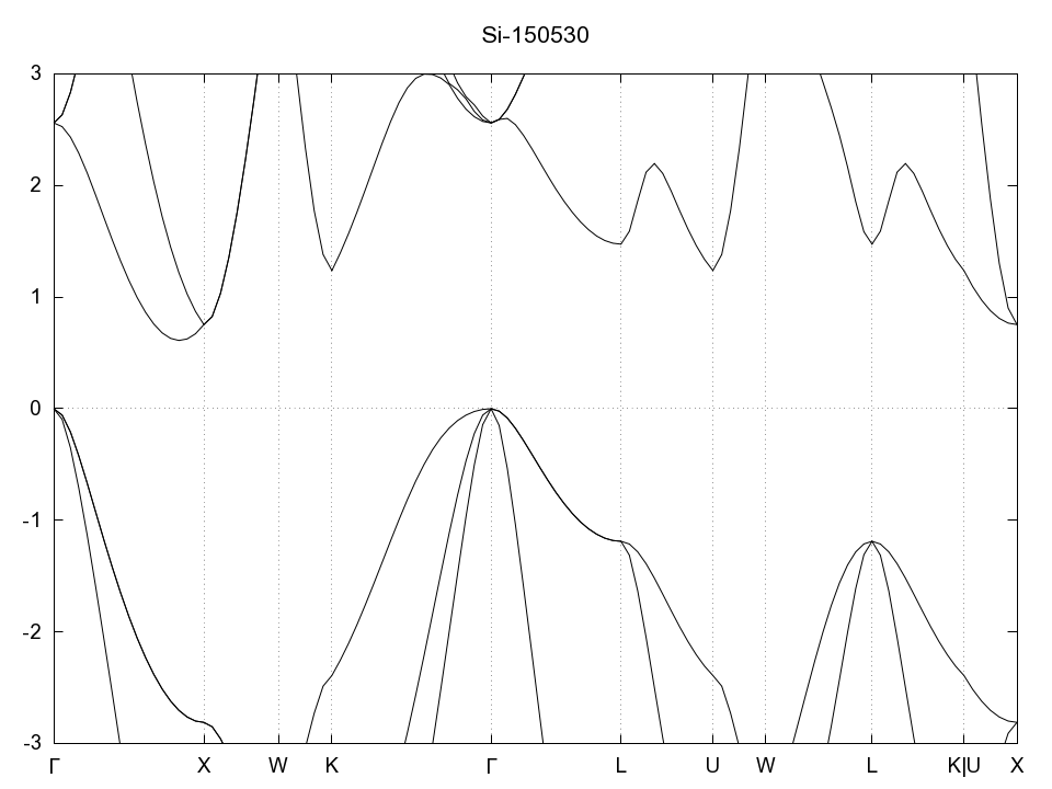
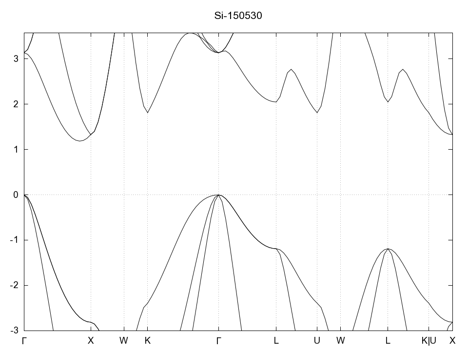
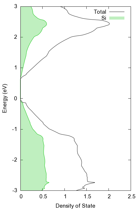
Si is a typical example of semiconductor. Therefore, we calculate all properties supported by AMP2in this example.
Optimized structure (/Results/POSCAR_rlx_GGA)
relaxed poscar
1.000000000
    0.0    2.73243086189    2.73243086189
    2.73243086189    -0.0    2.73243086189
    2.73243086189    2.73243086189    0.0
    Si
    2
Selective dynamics
Direct
    0.5    0.5    0.5  T  T  T ! Si1
    0.75    0.75    0.75  T  T  T ! Si1
Band gap (/Results/band_gap_GGA.log)
Band gap:      0.612 eV (Indirect)

VBM: 0.0  0.0  0.0   :      5.649 eV
CBM: 0.4166667  0.0  0.4166667   :      6.261 eV

nVBM: 4  spin: 1
nCBM: 5  spin: 1
Band structure (/Results/band_GGA.png and /Results/band_GGA.pdf)
Band gap from HSE@PBE (/Results/band_hybrid_GGA.log)
Band gap:      1.187 eV (Indirect)

VBM: 0.0  0.0  0.0   :      5.289 eV
CBM: 0.4166667  0.0  0.4166667   :      6.477 eV

nVBM: 4  spin: 1
nCBM: 5  spin: 1
Corrected band structure (/Results/band_GGA_corrected.png and /Results/band_GGA_corrected.pdf)
Density of states (/Results/dos_GGA.log)
Dielectric constant (/Results/dielectric_GGA.log)
Dielectric tensor (electronic contribution):
    12.936       0.000      -0.000
    0.000      12.936       0.000
    -0.000       0.000      12.936
Dielectric tensor (ionic contribution):
    0.000       0.000       0.000
    0.000      -0.000      -0.000
    0.000      -0.000       0.000

Dielectric constant diagonalization (electronic):     12.936     12.936     12.936
Dielectric constant diagonalization (ionic):      0.000     -0.000      0.000

Averaged static dielectric constant:     12.936
Effective mass of hole (/effective_mass_hole_GGA.log)
hole
    -0.266     -0.000     -0.000
    -0.000     -0.266     -0.000
    -0.000     -0.000     -0.266
Diagonalized effective mass:     -0.266     -0.266     -0.266
Effective mass of electron (/Results/effective_mass_hole_GGA.log)
electron
    0.287      0.000      0.000
    0.000      0.287      0.000
    0.000      0.000      0.287
Diagonalized effective mass:      0.287      0.287      0.287
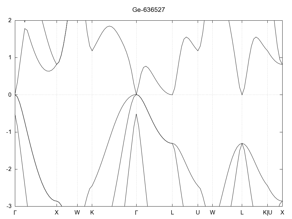
Ge
Ge is a well-known semiconductor with metallic band structure in conventional DFT schemes like LDA and PBE. In AMP2, however, we can obtain the reliable band gap and band structure due to the band gap correction scheme. In this example, we calculate corrected band structure.
Band gap (/Results/band_gap_GGA.log)
This system is metallic.
! If it is not hybrid calculation, additional search is required for hybrid calculation.
Band structure (/Results/band_GGA.png and /Results/band_GGA.pdf)
Band gap from HSE@PBE (/Results/band_hybrid_GGA.log)
Band gap:      0.161 eV (Direct)

VBM: 0.0  0.0  0.0   :      2.875 eV
CBM: 0.0  0.0  0.0   :      3.036 eV

nVBM: 4  spin: 1
nCBM: 5  spin: 1
Corrected band structure (/Results/band_GGA_corrected.png and /Results/band_GGA_corrected.pdf)

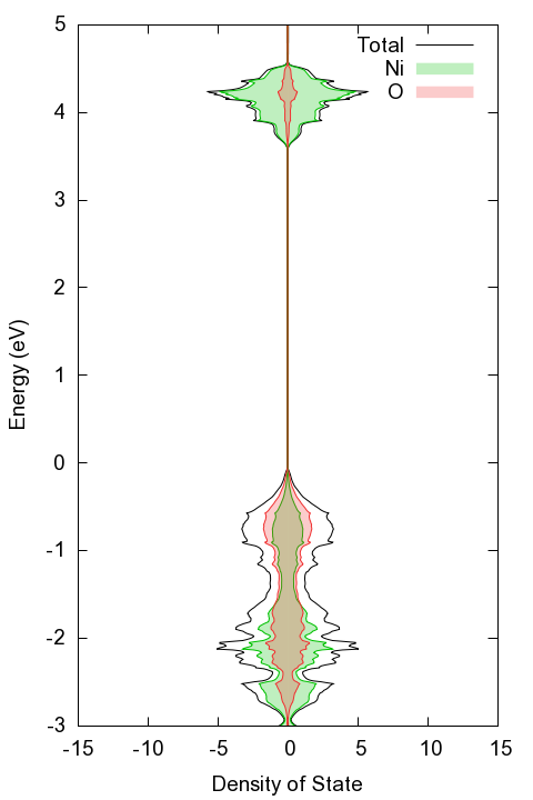
NiO
NiO is one of the antiferromagnetic materials. In this example, we show the most stable magnetic spin ordering for NiO and its electronic configurations (band strucrue and density of states).
Optimized structure (/Results/POSCAR_rlx_GGA)
relaxed poscar
1.000000000
    1.47786935879    0.853248272122    4.82278497551
    -1.47786935879    0.853248272122    4.82278497551
    0.0    -1.70649654425    4.82278497551
    Ni    O
    2    2
Selective dynamics
Direct
    0.5    0.5    0.5  T  T  T ! Ni1_up
    -0.0    -0.0    0.0  T  T  T ! Ni1_down
    0.750000037602    0.750000037602    0.750000037602  T  T  T ! O1
    0.249999962398    0.249999962398    0.249999962398  T  T  T ! O1
Band gap (/Results/band_gap_GGA.log)
Band gap:      3.433 eV (Indirect)

VBM: 0.5  0.5  0.5   :      6.242 eV
CBM: 0.0  0.0  0.0   :      9.675 eV

nVBM: 16  spin: 1
nCBM: 17  spin: 2
Band structure (/Results/band_GGA.png and /Results/band_GGA.pdf)

Density of states (/Results/dos_GGA.log)